- 您现在的位置:买卖IC网 > Sheet目录2004 > LTC1661IMS8#TRPBF (Linear Technology)IC D/A CONV 10BIT MICRPWR 8-MSOP
LTC1661
4
1661fa
TIMING CHARACTERISTICS The
l
denotes the specifications which apply over the full operating temperature
range, otherwise specifications are at TA = 25°C.
SYMBOL
PARAMETER
CONDITIONS
MIN
TYP
MAX
UNITS
VCC = 2.7V to 5.5V
t1
DIN Valid to SCK Setup
(Note 6)
l
60
ns
t2
DIN Valid to SCK Hold
(Note 6)
l
0
ns
t3
SCK High Time
(Note 6)
l
50
ns
t4
SCK Low Time
(Note 6)
l
50
ns
t5
CS/LD Pulse Width
(Note 6)
l
100
ns
t6
LSB SCK High to CS/LD High
(Note 6)
l
50
ns
t7
CS/LD Low to SCK High
(Note 6)
l
30
ns
t9
SCK Low to CS/LD Low
(Note 6)
l
0
ns
t11
CS/LD High to SCK Positive Edge
(Note 6)
l
30
ns
SCK Frequency
Square Wave (Note 6)
l
10
MHz
Note 1: Stresses beyond those listed under Absolute Maximum Ratings
may cause permanent damage to the device. Exposure to any Absolute
Maximum Rating condition for extended periods may affect device
reliability and lifetime.
Note 2: Nonlinearity and monotonicity are defined from code 20 to code
1023 (full scale). See Applications Information.
Note 3: Digital inputs at 0V or VCC.
Note 4: Load is 10k
Ω in parallel with 100pF.
Note 5: VCC = VREF = 5V. DAC switched between 0.1VFS and 0.9VFS,
i.e., codes k = 102 and k = 922.
Note 6: Guaranteed by design and not subject to test.
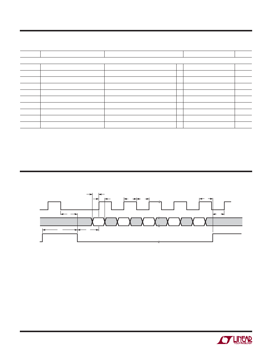
TIMING DIAGRAM
DIN
CS/LD
SCK
A3
A2
1661 TD
A1
X1
X0
t2
t9
t11
t5
t7
t6
t1
t3
t4
发布紧急采购,3分钟左右您将得到回复。
相关PDF资料
LTC1662IN8#PBF
IC D/A CONV 10BIT MICRPWR 8-DIP
LTC1663-1CS5#TRM
IC DAC 10BIT R-R TSOT23-5
LTC1664IN
IC DAC 10BIT QUAD MICRPWR 16DIP
LTC1667CG#PBF
IC D/A CONV 14BIT 50MSPS 28-SSOP
LTC1686IS8#TRPBF
IC TXRX RS485 PREC DELAY 8-SOIC
LTC1688IS
IC DVR 100MBPS RS485 QUAD 16SOIC
LTC1690IS8#TRPBF
IC RCVR/DVR PAIR LOW PWR 8-SOIC
LTC1740IG#TRPBF
IC ADC 14BIT 6MSPS 36SSOP
相关代理商/技术参数
LTC1661IN8
功能描述:IC D/A CONV 10BIT MICRPWR 8-DIP RoHS:否 类别:集成电路 (IC) >> 数据采集 - 数模转换器 系列:- 产品培训模块:Data Converter Fundamentals
DAC Architectures 设计资源:Unipolar, Precision DC Digital-to-Analog Conversion using AD5450/1/2/3 8-14-Bit DACs (CN0052)
Precision, Bipolar, Configuration for AD5450/1/2/3 8-14bit Multiplying DACs (CN0053)
AC Signal Processing Using AD5450/1/2/3 Current Output DACs (CN0054)
Programmable Gain Element Using AD5450/1/2/3 Current Output DAC Family (CN0055)
Single Supply Low Noise LED Current Source Driver Using a Current Output DAC in the Reverse Mode (CN0139) 标准包装:10,000 系列:- 设置时间:- 位数:12 数据接口:DSP,MICROWIRE?,QSPI?,串行,SPI? 转换器数目:1 电压电源:单电源 功率耗散(最大):- 工作温度:-40°C ~ 125°C 安装类型:表面贴装 封装/外壳:SOT-23-8 薄型,TSOT-23-8 供应商设备封装:TSOT-23-8 包装:带卷 (TR) 输出数目和类型:1 电流,单极;1 电流,双极 采样率(每秒):2.7M
LTC1661IN8#PBF
功能描述:IC D/A CONV 10BIT MICRPWR 8-DIP RoHS:是 类别:集成电路 (IC) >> 数据采集 - 数模转换器 系列:- 产品培训模块:Data Converter Fundamentals
DAC Architectures 设计资源:Unipolar, Precision DC Digital-to-Analog Conversion using AD5450/1/2/3 8-14-Bit DACs (CN0052)
Precision, Bipolar, Configuration for AD5450/1/2/3 8-14bit Multiplying DACs (CN0053)
AC Signal Processing Using AD5450/1/2/3 Current Output DACs (CN0054)
Programmable Gain Element Using AD5450/1/2/3 Current Output DAC Family (CN0055)
Single Supply Low Noise LED Current Source Driver Using a Current Output DAC in the Reverse Mode (CN0139) 标准包装:10,000 系列:- 设置时间:- 位数:12 数据接口:DSP,MICROWIRE?,QSPI?,串行,SPI? 转换器数目:1 电压电源:单电源 功率耗散(最大):- 工作温度:-40°C ~ 125°C 安装类型:表面贴装 封装/外壳:SOT-23-8 薄型,TSOT-23-8 供应商设备封装:TSOT-23-8 包装:带卷 (TR) 输出数目和类型:1 电流,单极;1 电流,双极 采样率(每秒):2.7M
LTC1662CMS8
功能描述:IC DAC 10BIT DUAL ULT LPWR 8MSOP RoHS:否 类别:集成电路 (IC) >> 数据采集 - 数模转换器 系列:- 产品培训模块:Data Converter Fundamentals
DAC Architectures 设计资源:Unipolar, Precision DC Digital-to-Analog Conversion using AD5450/1/2/3 8-14-Bit DACs (CN0052)
Precision, Bipolar, Configuration for AD5450/1/2/3 8-14bit Multiplying DACs (CN0053)
AC Signal Processing Using AD5450/1/2/3 Current Output DACs (CN0054)
Programmable Gain Element Using AD5450/1/2/3 Current Output DAC Family (CN0055)
Single Supply Low Noise LED Current Source Driver Using a Current Output DAC in the Reverse Mode (CN0139) 标准包装:10,000 系列:- 设置时间:- 位数:12 数据接口:DSP,MICROWIRE?,QSPI?,串行,SPI? 转换器数目:1 电压电源:单电源 功率耗散(最大):- 工作温度:-40°C ~ 125°C 安装类型:表面贴装 封装/外壳:SOT-23-8 薄型,TSOT-23-8 供应商设备封装:TSOT-23-8 包装:带卷 (TR) 输出数目和类型:1 电流,单极;1 电流,双极 采样率(每秒):2.7M
LTC1662CMS8#PBF
功能描述:IC D/A CONV 10BIT MICRPWR 8-MSOP RoHS:是 类别:集成电路 (IC) >> 数据采集 - 数模转换器 系列:- 产品培训模块:Data Converter Fundamentals
DAC Architectures 设计资源:Unipolar, Precision DC Digital-to-Analog Conversion using AD5450/1/2/3 8-14-Bit DACs (CN0052)
Precision, Bipolar, Configuration for AD5450/1/2/3 8-14bit Multiplying DACs (CN0053)
AC Signal Processing Using AD5450/1/2/3 Current Output DACs (CN0054)
Programmable Gain Element Using AD5450/1/2/3 Current Output DAC Family (CN0055)
Single Supply Low Noise LED Current Source Driver Using a Current Output DAC in the Reverse Mode (CN0139) 标准包装:10,000 系列:- 设置时间:- 位数:12 数据接口:DSP,MICROWIRE?,QSPI?,串行,SPI? 转换器数目:1 电压电源:单电源 功率耗散(最大):- 工作温度:-40°C ~ 125°C 安装类型:表面贴装 封装/外壳:SOT-23-8 薄型,TSOT-23-8 供应商设备封装:TSOT-23-8 包装:带卷 (TR) 输出数目和类型:1 电流,单极;1 电流,双极 采样率(每秒):2.7M
LTC1662CMS8#TR
功能描述:IC DAC 10BIT DUAL ULT LPWR 8MSOP RoHS:否 类别:集成电路 (IC) >> 数据采集 - 数模转换器 系列:- 产品培训模块:Data Converter Fundamentals
DAC Architectures 设计资源:Unipolar, Precision DC Digital-to-Analog Conversion using AD5450/1/2/3 8-14-Bit DACs (CN0052)
Precision, Bipolar, Configuration for AD5450/1/2/3 8-14bit Multiplying DACs (CN0053)
AC Signal Processing Using AD5450/1/2/3 Current Output DACs (CN0054)
Programmable Gain Element Using AD5450/1/2/3 Current Output DAC Family (CN0055)
Single Supply Low Noise LED Current Source Driver Using a Current Output DAC in the Reverse Mode (CN0139) 标准包装:10,000 系列:- 设置时间:- 位数:12 数据接口:DSP,MICROWIRE?,QSPI?,串行,SPI? 转换器数目:1 电压电源:单电源 功率耗散(最大):- 工作温度:-40°C ~ 125°C 安装类型:表面贴装 封装/外壳:SOT-23-8 薄型,TSOT-23-8 供应商设备封装:TSOT-23-8 包装:带卷 (TR) 输出数目和类型:1 电流,单极;1 电流,双极 采样率(每秒):2.7M
LTC1662CMS8#TRPBF
功能描述:IC D/A CONV 10BIT MICRPWR 8-MSOP RoHS:是 类别:集成电路 (IC) >> 数据采集 - 数模转换器 系列:- 产品培训模块:Data Converter Fundamentals
DAC Architectures 设计资源:Unipolar, Precision DC Digital-to-Analog Conversion using AD5450/1/2/3 8-14-Bit DACs (CN0052)
Precision, Bipolar, Configuration for AD5450/1/2/3 8-14bit Multiplying DACs (CN0053)
AC Signal Processing Using AD5450/1/2/3 Current Output DACs (CN0054)
Programmable Gain Element Using AD5450/1/2/3 Current Output DAC Family (CN0055)
Single Supply Low Noise LED Current Source Driver Using a Current Output DAC in the Reverse Mode (CN0139) 标准包装:10,000 系列:- 设置时间:- 位数:12 数据接口:DSP,MICROWIRE?,QSPI?,串行,SPI? 转换器数目:1 电压电源:单电源 功率耗散(最大):- 工作温度:-40°C ~ 125°C 安装类型:表面贴装 封装/外壳:SOT-23-8 薄型,TSOT-23-8 供应商设备封装:TSOT-23-8 包装:带卷 (TR) 输出数目和类型:1 电流,单极;1 电流,双极 采样率(每秒):2.7M
LTC1662CN8
功能描述:IC DAC 10BIT DUAL ULT LPWR 8DIP RoHS:否 类别:集成电路 (IC) >> 数据采集 - 数模转换器 系列:- 产品培训模块:Data Converter Fundamentals
DAC Architectures 设计资源:Unipolar, Precision DC Digital-to-Analog Conversion using AD5450/1/2/3 8-14-Bit DACs (CN0052)
Precision, Bipolar, Configuration for AD5450/1/2/3 8-14bit Multiplying DACs (CN0053)
AC Signal Processing Using AD5450/1/2/3 Current Output DACs (CN0054)
Programmable Gain Element Using AD5450/1/2/3 Current Output DAC Family (CN0055)
Single Supply Low Noise LED Current Source Driver Using a Current Output DAC in the Reverse Mode (CN0139) 标准包装:10,000 系列:- 设置时间:- 位数:12 数据接口:DSP,MICROWIRE?,QSPI?,串行,SPI? 转换器数目:1 电压电源:单电源 功率耗散(最大):- 工作温度:-40°C ~ 125°C 安装类型:表面贴装 封装/外壳:SOT-23-8 薄型,TSOT-23-8 供应商设备封装:TSOT-23-8 包装:带卷 (TR) 输出数目和类型:1 电流,单极;1 电流,双极 采样率(每秒):2.7M
LTC1662CN8#PBF
功能描述:IC D/A CONV 10BIT MICRPWR 8-DIP RoHS:是 类别:集成电路 (IC) >> 数据采集 - 数模转换器 系列:- 标准包装:2,400 系列:- 设置时间:- 位数:18 数据接口:串行 转换器数目:3 电压电源:模拟和数字 功率耗散(最大):- 工作温度:-40°C ~ 85°C 安装类型:表面贴装 封装/外壳:36-TFBGA 供应商设备封装:36-TFBGA 包装:带卷 (TR) 输出数目和类型:* 采样率(每秒):*